ΑΙhub.org
Deep learning-guided surface characterization for autonomous fabrication
The semiconductor industry as we know it is facing a critical roadblock that will lead to the end of Moore’s law. As transistors continue to shrink, quantum effects have a significant negative consequence on their operation. As such, the development of “beyond CMOS devices” has begun.
The push for devices that are cheaper, smaller, and faster has led to the use of scanning probe fabrication. One of the first examples of such a technique was IBM’s video “A boy and his atom”, where CO molecules were moved along a Cu surface using a sharp metallic tip. Limitations in the thermal stability of using metal surfaces for device fabrication lead to the development of hydrogen lithography. Using a scanning probe tip, hydrogen can be selectively removed from a silicon surface at atomic resolution (roughly 0.3 nm) providing thermal stability as well as compatibility with today’s enormous silicon-based transistor fabrication infrastructure.
Hydrogen lithography is used for the viable creation of such “beyond CMOS devices” as quantum computers, single atom transistors, and Binary Atomic Silicon Logic. The latter is pictured above where the absence of a hydrogen atom creates a quantum dot. These quantum dots are capable of representing binary information through the presence or absence of a single electron, drastically reducing the predicted energy consumption and spatial requirements of today’s modern transistors.
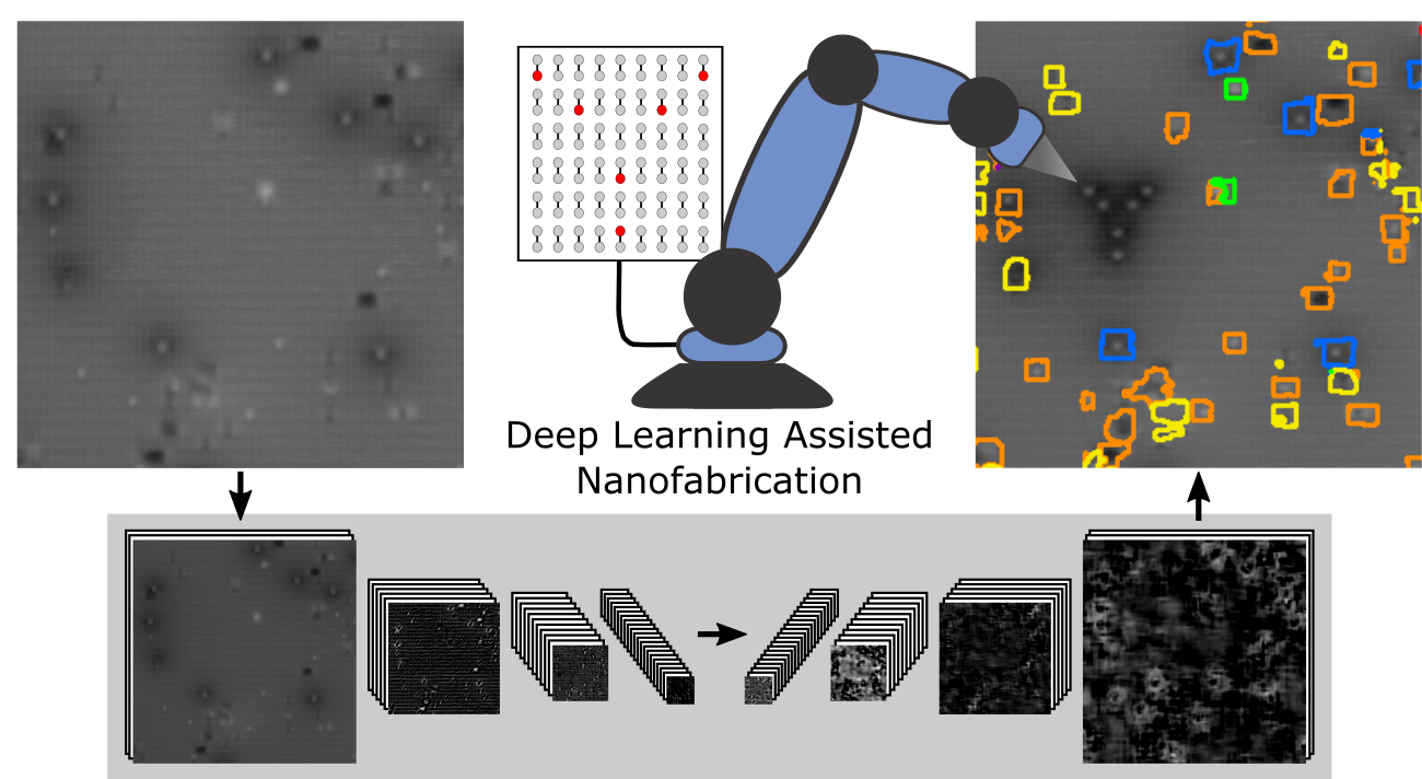
One of the leading issues with this fabrication technique is that at present, it is not scalable. The complexity of the surface requires constant monitoring to assess the quality of both the scanning probe tip and the silicon surface. By employing deep learning methods through the use of convolutional neutral networks (CNNs), we have been able to automate the entire fabrication process. Networks used for assessing tip quality must only distinguish between a “good” and “bad” tip which subsequently triggers an in situ tip reconditioning algorithm if needed. The surface quality is assessed using a greater number of factors, requiring a more complicated scheme.
A perfect surface consists of a perfectly flat silicon surface where each surface silicon atom bonds to a single hydrogen atom. In actuality there are numerous different configurations such as missing silicon atoms, additional hydrogens, or even residual water molecules, all of which make a specific lattice site unable to host a quantum dot. The formation of such defects can only be controlled to a certain degree, and ultimately depends on their thermodynamic probabilities of formation. By developing a CNN capable of semantic segmentation, we have been able to fully automate the surface quality assessment. Using seven different classes, the network is capable of distinguishing between defects that can alter the device behaviour, prevent the connection of additional devices, or simply prevent a single quantum dot from being fabricated. With a full understanding of where the defects exist on the surface, the most viable area of the surface can be calculated which allows for an automated hydrogen lithography process to fabricate these quantum dot devices in an effectively defect-free area.
Without the need for a single user to constantly monitor tip and surface quality, this allows for a fully scalable process where a single user could now monitor hundreds of machines providing a potential roadmap for the commercial fabrication of “beyond CMOS devices” using scanning probe systems.
Read the research articles
Deep learning-guided surface characterization for autonomous hydrogen lithography
Mohammad Rashidi, Jeremiah Croshaw, Kieran Mastel, Marcus Tamura, Hedieh Hosseinzadeh and Robert A Wolkow
Mach. Learn. Sci. Technol. 1, 025001 (2020)
Autonomous Scanning Probe Microscopy in situ Tip Conditioning through Machine Learning
Mohammad Rashidi and Robert A. Wolkow
ACS Nano 12, 5185–5189 (2018)

AUAI is supported by: